Parametrizable Hybrid Stack-Register
Processor as VHDL Soft-Intellectual Property Module
Students project at the Integrated Systems Laboratory of the
Swiss Federal Institute of Technology, Zurich, Switzerland
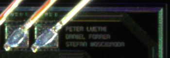
Students: Peter Luethi, Daniel Forrer, Stefan Moscibroda
Assistants: Thomas Roewer, Manfred Stadler
Design, Verification & Integration: October 1999 -
February 2000
Hardware Testing & Measurements: May - July 2000
Overview
Architecture
Highlights
Parameters
Test integration
Technical data
Conclusions
Acknowledgements
Publications
The design of integrated circuits is currently subject to
extensive changes. Until now, project-specific code has been
written for every new design. This results in highly optimized
code for the target application, but also leads to increased
development time, especially for large designs. Since time to
market becomes more and more important, the traditional way of
designing integrated circuits has to be altered to get the
efficiency as before. As the complexity of circuits increases,
there is urgent need for new design methodologies, which allows
fast development of demanding applications up to complete
system-on-a-chip integrations.
One possibility to cope with this efficiency problem is the use
of so called Intellectual Property (IP) Modules or
Virtual Components (VC). This method is based on the idea
to put pre-defined functional blocks together to a complete
system. Quick and easy adaptations on the reusable blocks speeds
up system design and provides more time for thorough testing, an
important issue in cost-intensive chip design.
During this students project, there should now be developed a
parametrizable RISC processor in VHDL from scratch. The processor
has to be parametrizable in a wide range and has to manage medium
to high interrupt loads without any problems. A convenient
testbench environment is also required to obtain the ability for
quick implementation of the processor IP in a system-on-a-chip
(SOC) application.
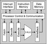 First
we had to figure out which pipeline depth our processor
should obtain. The answer of this question is always crucial
for both overall processor performance and implementation
complexity. To keep the complexity within reasonable bounds
and allow for fast interrupt launch with minimum latency, we
finally decided to choose a classic four stage pipeline
consisting of Instruction Fetch, Instruction
Decode, Execute and WriteBack stage. First
we had to figure out which pipeline depth our processor
should obtain. The answer of this question is always crucial
for both overall processor performance and implementation
complexity. To keep the complexity within reasonable bounds
and allow for fast interrupt launch with minimum latency, we
finally decided to choose a classic four stage pipeline
consisting of Instruction Fetch, Instruction
Decode, Execute and WriteBack stage. |
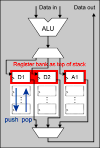 To
meet the demanding requirements of managing high interrupt
loads and being parametrizable, we have decided to combine
the advantages of a stack architecture with the ones of a
register-based approach. Therefore, the general purpose
registers of our processor are implemented as top of stack
registers (red area). In case of an interrupt, precious
processing time for context switch can be saved by just
pushing the current register contents on the stack. The
maximum interrupt latency achieved by our architecture is two
clock cycles, but in most situations, we are able to launch
the interrupt service routine within one clock cycle. To
obtain maximum processor performance, neither the pipeline is
ever flushed nor any no-operation cycles are performed. On
branchs, we use delayed-branch execution of one instruction
for not wasting any cycles. To
meet the demanding requirements of managing high interrupt
loads and being parametrizable, we have decided to combine
the advantages of a stack architecture with the ones of a
register-based approach. Therefore, the general purpose
registers of our processor are implemented as top of stack
registers (red area). In case of an interrupt, precious
processing time for context switch can be saved by just
pushing the current register contents on the stack. The
maximum interrupt latency achieved by our architecture is two
clock cycles, but in most situations, we are able to launch
the interrupt service routine within one clock cycle. To
obtain maximum processor performance, neither the pipeline is
ever flushed nor any no-operation cycles are performed. On
branchs, we use delayed-branch execution of one instruction
for not wasting any cycles.A striking argument against a pure stack processor was the need for compiler-compatibility: A compiler for a stack architecture is difficult to implement, because it always needs to trace the exact position of each register. As a consequence, the entire stack has to be controlled by software ("push" & "pop" instructions). |
|
One slight disadvantage of our architecture is the large
chip area taken by the stacks. But this can be omitted by
implementing an interface from the top of stack registers
to an on-chip RAM and putting the main part of the stack
contents to the RAM. It will result in more control logic
and maybe in lower performance, unless the user builds a
complex control logic to cope with the slow RAM. This way
to save chip area is only preferable on large
parameterizations. |
 |
|
||||||||||||
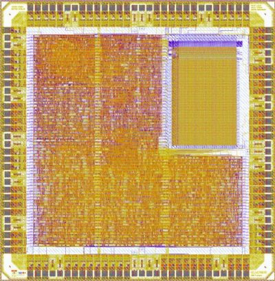
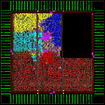
| Visualization of Functional
Regions Screenshot of our RISC Processor and its various Blocks in Silicon Ensemble. Picture courtesy of Peter Luethi |
|||||||||||||
|
Screenshot taken from Cadence DFII |
We have decided to implement the data memory as on-chip static
RAM (SRAM) and to leave the instruction memory off-chip to get
the ability to verify the maximum processor speed on the tester.
The data width has been set to 16 bit, the on-chip data memory
has a size of 1024 x 16 bit.
The entire physical testability has been met with 11 scan pathes
through the processor core (full-scan) and the complete isolation
and extern accessibility of the embedded SRAM. For the SRAM, we
have written an extern alternating chess pattern test program to
check the correct physical integration.
The whole back-end design downto the final seal-ring has also
been carried out by ourself: As a consequence we got a thorough
understanding of the back-end design-flow and back-annotation
with Silicon Ensemble 5.3, Pearl and Cadence DesignFramework
II.
|
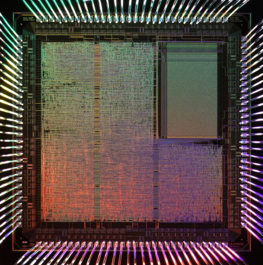
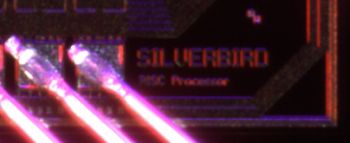
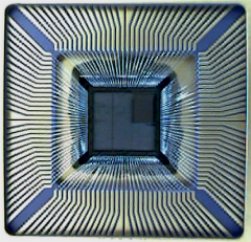
Chip Photography of our "SILVERBIRD" RISC
Processor |
 |
 |
|
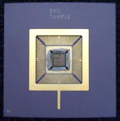
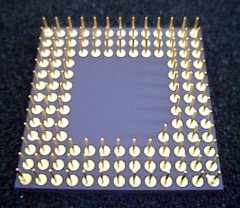
| Package of our "SILVERBIRD"
Processor Ceramic Pin Grid Array (CPGA) with 120 pins |
||
 |
Last updated referring to latest measurements : 14th July 2000
| Process |
| 0.6 um 3 LM CMOS Process |
| 5 Volts, Austria Micro Systems AMS HK 3.20 |
| Configuration | ||||
| Instruction Memory: | off-chip | Number of Data Registers: | 12 | |
| Data Memory: | on-chip | Number of Address Registers: | 4 | |
| Instruction Memory Address Width: | 11 bit | Stack Depth: | 4 | |
| Data Width: | 16 bit | Return Address Stack Depth: | 20 | |
| Data Memory Address Width: | 10 bit | on-chip DMem (SRAM): | 1024 x 16 bit | |
| Performance (5 V, 25°C ambient temperature) | |
| Max. Operating Frequency: | 121.5 MHz |
| Max. Throughput: | 121.5 MIPS |
| Interrupt Latency: | max. 2 Tclk = 16.46 ns @ 121.5 MHz |
| Core Power Consumption: | 288 mA @ 121.5 MHz, 5 V |
| 19.7 mA @ 21.9 MHz, 1.9 V | |
| Power / MIPS: | 11.85 mW / MIPS @ 121.5 MHz, 5 V |
| 1.7 mW / MIPS @ 21.9 MHz, 1.9 V | |
| Dimensions | |
| Chip Size: | 4.6 x 4.6 mm |
| Chip Area: | 21.16 mm² |
| Core Size: | 3.7 x 3.7 mm |
| Core Area: | 13.69 mm² |
| Number of Pins: | 120 including power supply |
| Package: | 120 pin CPGA |
| Statistics | |
| Number of Standard Cells: | 8712 |
| Number of Transistors (without SRAM): | 104'657 |
| Estimated Number of Transistors with SRAM: | ~ 230'000 |
| Standard Cell Usage: | 792 Cells / mm² |
| Transistor Usage (without SRAM): | 10'208 Transistors / mm² |
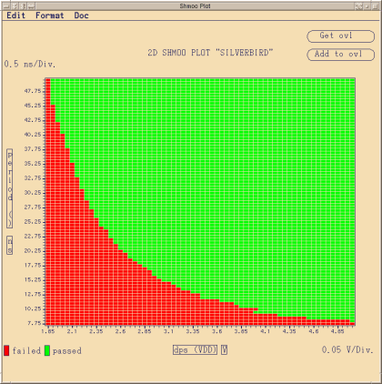
Voltage - Operating Frequency - Shmoo
Plot |
We have developed an embedded processor IP-Module which is highly adaptable in both functionality and configuration. This was achieved by separating the processor core and the system interfaces. The hybrid stack-register processor is excellently suited for applications with high interrupt loads. There is a convenient verification flow covering automatically the configuration of the processor.
Our team has been successfully introduced to the entire design-flow (system engineering, front-end design, back-end design & back-annotation) of an ASIC with this huge student project. We had to cope with the difficulties of system engineering, project scheduling and the complexity of the design tools. The callenge to design a perfect solution and the possibility to realize such a project already during our study encouraged us keeping up our hard work even during the christmas holidays. As a consequence, we could finally present an outstanding result and obtained the highest grade for it.
"It's not a disgrace, if you can't achieve a perfect solution. But it is, if you don't even try."
Special thanks to:
| My team members: Daniel Forrer and Stefan
Moscibroda. Was a great project beside a huge amount of work. Thanks, guys! |
|
| Our assistants: Thomas Roewer and Manfred Stadler of the Integrated Systems Laboratory, ETH Zurich | |
| Integrated Systems Laboratory of the Swiss Federal Institute of Technology, Zurich, Switzerland and KTI (Swiss Commission for Technology and Innovations) for funding this project. |
| Parametrizable Hybrid Stack-Register Processor as Soft Intellectual Property Module |
| Paper about our "SILVERBIRD" Processor Soft
IP-Module written for the 13th Annual IEEE International ASIC/SOC Conference 2000, Washington D.C., Virginia USA, 13th - 16th September 2000 |
Last updated: 2006/01/15
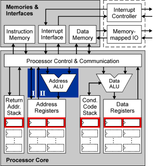 Our solution provides a fix amount of
general purpose registers for every interrupt level (red
area). The whole stack control is done by the processor
itself and requires no software-based "push" and "pop"
operations. This organization is easy to support by a
high-level compiler since it does not have to control the
stack at all.
Our solution provides a fix amount of
general purpose registers for every interrupt level (red
area). The whole stack control is done by the processor
itself and requires no software-based "push" and "pop"
operations. This organization is easy to support by a
high-level compiler since it does not have to control the
stack at all.