VLSI Circuits for MIMO Preprocessing,
Hartung-Gorre, 2010, Ph.D. dissertation, ETH Zurich, Zurich, Switzerland,
222 pages, € 64,00
ISBN-10: 3-86628-295-8
ISBN-13: 978-3-86628-295-7
Excerpt with ToC, Ordering Information
Research Activities in the Field of
MIMO Wireless Communication
Ph.D. Thesis
General
Information
Abstract
About the Author
Keywords
The Research Project
The MMSE-SQRD ASIC
The real-time 4x4 MIMO-OFDM
Testbed
WinTech'08 Live
Demonstration Preparation
WinTech'08 Live
Demonstration Contest
ISCAS'09 Live Demonstration
Contest
Testbed Deployment of the MMSE-SQRD
ASIC
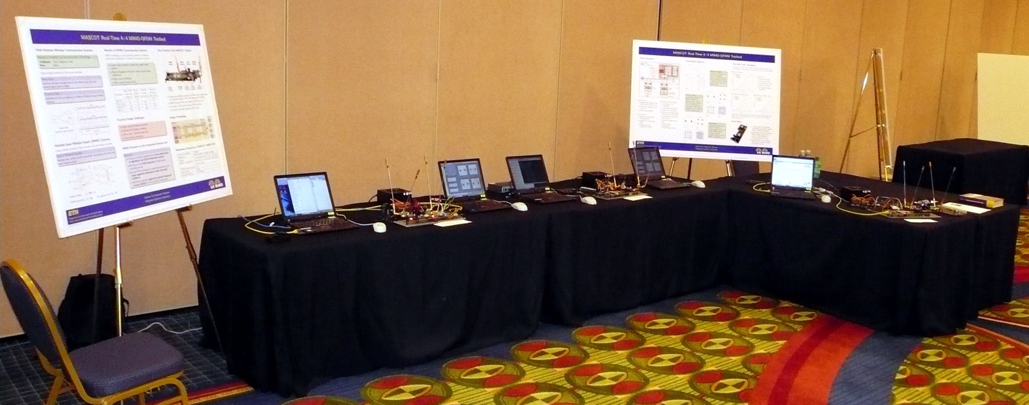
Illustrating Material / Posters
|
|
Peter Jan Lüthi, VLSI Circuits for MIMO Preprocessing, Hartung-Gorre, 2010, Ph.D. dissertation, ETH Zurich, Zurich, Switzerland, 222 pages, € 64,00 ISBN-10: 3-86628-295-8 ISBN-13: 978-3-86628-295-7 Excerpt with ToC, Ordering Information |
The latest mobile applications and the growing number of
wireless users are increasing the demand for high-throughput
wireless access solutions. Multiple-input multiple-output (MIMO)
technology combined with orthogonal frequency-division
multiplexing (OFDM) constitute today's most promising approach to
exploit the limited radio frequency resources in a highly
efficient way. Unfortunately, the adoption of these technologies
significantly increases the signal processing complexity, what
ultimately calls for dedicated very-large scale integration
(VLSI) circuits. At system-level, careful evaluation of MIMO
preprocessing aspects offers great opportunities for lowering
MIMO detection complexity. This work focuses on VLSI circuits for
MIMO preprocessing, with emphasis on QR decomposition-based
architectures, and contains considerations for joint algorithmic
and architectural optimizations. Several architectures have been
realized as integrated circuits, including one proving its full
operational capabilities by being successfully deployed to a
real-time MIMO-OFDM testbed.
Peter Jan Lüthi was born in Schlieren, Switzerland, in
1977. He received his diploma degree in electrical engineering
from the ETH Zurich, Switzerland, in 2001. In the same year, he
joined Advanced Micro Devices (AMD) in order to work on
HyperTransport and PCI verification and performance enhancements.
In late 2003, he started his doctoral studies at the Integrated
Systems Laboratory of the ETH Zurich, working on digital signal
processing and integrated circuit design for MIMO wireless
communication.
MIMO preprocessing, V-BLAST, sorted QR decomposition (SQRD),
MMSE, Givens rotations, CORDIC, digital signal processing, VLSI
circuits, ASIC
The aim of the research project I was involved in during my
Ph.D. study was the design, implementation and demonstration of
suitable algorithms for MIMO wireless communication and its
assessment with respect to implementation complexity and
practical performance. Selected algorithms were implemented in a
real-time 4x4 MIMO-OFDM testbed and demonstrated under real-world
conditions.
In short, my activities in this research project generated the
following research contributions:
Here are few impressions of one of my application-specific integrated circuits (ASIC), which implements an algorithm called minimum mean squared error (MMSE) sorted QR decomposition (SQRD).
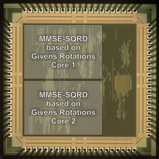 |
| Chip micrograph of the dual-core
MMSE-SQRD ASIC based on Givens rotations in UMC 0.18um
1P/6M CMOS technology. Both cores operate on the same I/O
interface in an interleaved fashion and double the
performance compared to single core operation, without
incurring penalties due to I/O limitations. |
 |
| A tribute to the ingenious CORDIC
circuit invented in 1959 by Jack E. Volder and the powerful
and efficient Intel Core architecture being popular at the
time of engineering my ASIC: MMSE-SQRD V2 -
"CORDIC 2 Duo - Do More" I hope, the legal department of Intel Corp. won't sue me... |
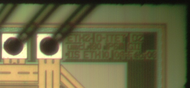 |
| ID of the MMSE-SQRD V2 ASIC: ETHZ D-ITET DZ, umcL180 1P6M GII, IIS ETH10 09-Feb-08 |
The initial MMSE-SQRD ASIC was taped out on February 26, 2007,
in UMC 0.18um 1P/6M CMOS technology. The purpose of two ASIC
integrations in the same technology was to assess any differences
in physical integration and manufacturing concerning the maximum
clock frequency of the final circuits (post-layout timing vs.
actual silicon clock frequency).
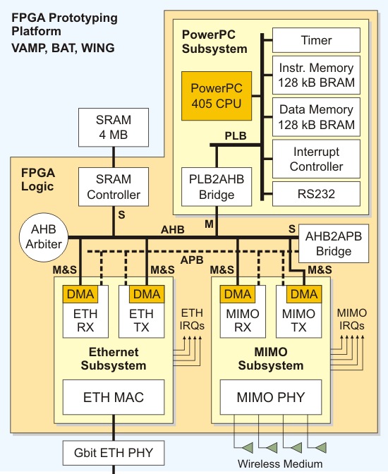
In the following, a brief overview of the 4x4 MIMO-OFDM
testbed with embedded real-time signal processing and MAC layer
handling is provided. In the end, the MIMO testbed was quite a
complex hardware-software architecture including FPGA and ASIC
resources, an embedded IBM PowerPC 405 RISC CPU (available as
hard macro cell in the XILINX Virtex-II Pro FPGAs) for handling
the MAC layer tasks, custom-designed 2.4 GHz RF circuitry
for wireless communication, and a Gigabit Ethernet device for
wired connectivity. Finally, we were able to stream movies and to
download files from the Internet across our real-time MIMO
prototyping system.
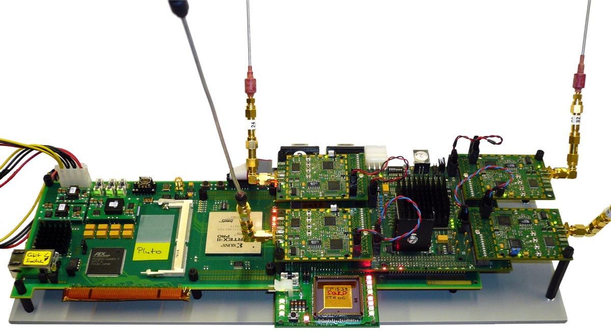 |
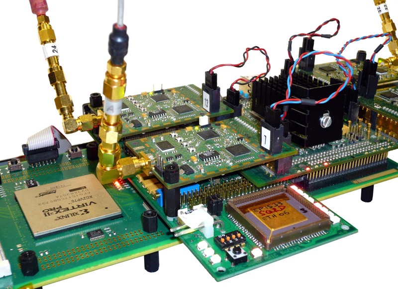
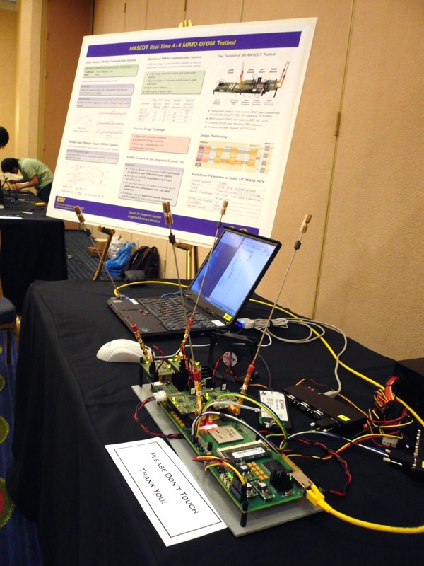
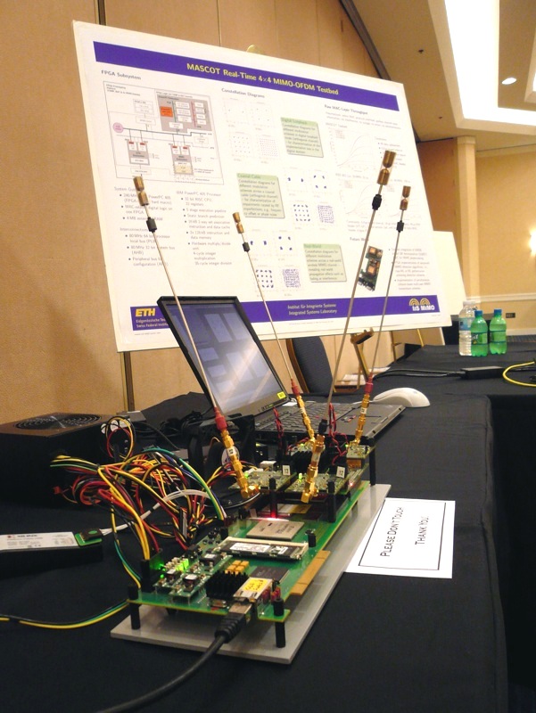
| One terminal of the real-time 4x4 MIMO-OFDM testbed consisting of two XILINX Virtex-II Pro (XC2VP70-5-ff1517) FPGAs, one XILINX Virtex-4 (XC4VSX55-10-ff1148) FPGA, and two MMSE-SQRD ASICs. Note that every board carries its unique identifier such as Mickey, Goofy, Donald, Dagobert, Gustav, Daisy, Minnie, and Pluto. |
 |
| Fully operational SQRD-based MIMO preprocessing with two dual-core MMSE-SQRD ASICs in the real-time 4x4 MIMO-OFDM testbed. One MMSE-SQRD ASIC is visible in front, the second ASIC is located underneath the two RF boards. The SQRD-based MIMO preprocessing resides in between channel estimation and MIMO processing. |
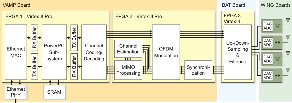 |
| Partitioning of the real-time 4x4
MIMO-OFDM testbed across three FPGAs and three
different types of prototyping boards. The boards were
named 'Virtex-II Pro astonishing multi-purpose' (VAMP)
board, and accordingly, BAT and WING boards. The VAMP board
was in charge of all baseband signal processing and MAC
layer tasks, the BAT board handled the digital front-end
signal processing, and the WING boards performed wireless
transmission and reception at 2.4 GHz. Not indicated here is the additional interface to the SQRD-based MIMO preprocessing, which resides in between channel estimation and MIMO processing and infers another PCB and two MMSE-SQRD ASICs. |
Having been invited to the third international workshop on Wireless Network Testbeds, Experimental Evaluation and Characterization (WiNTECH) and the associated live demonstration contest at the ACM International Conference on Mobile Computing and Networking (MobiCom) in San Francisco, CA, USA, we had to get the testbed equipment ready for take-off.
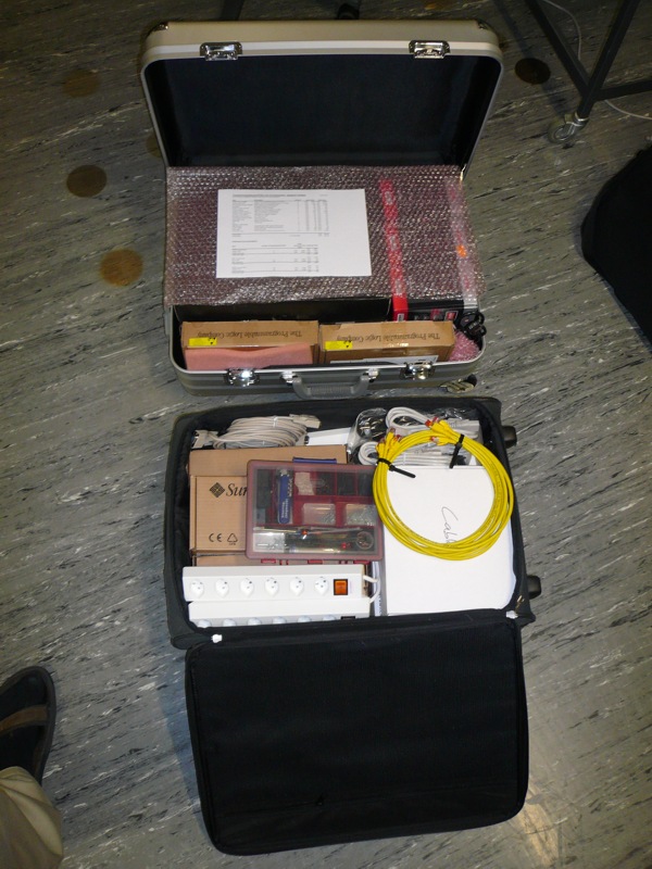 |
| The entire MIMO prototyping system
consisting of three terminals in two suitcases (without
laptops) ready for departure to San Francisco, CA, USA, in
September 2008. With respect to customs and the mandatory
Carnet A.T.A., the customs officers at JFK International
Airport were very friendly and, due to temporal coincidence
with the first successful proton collisions in the
Large
Hadron Collider (LHR) at CERN, quite amused
that again some Swiss carry some obscure equipment, which
would potentially provoke the formation of another black
hole... |
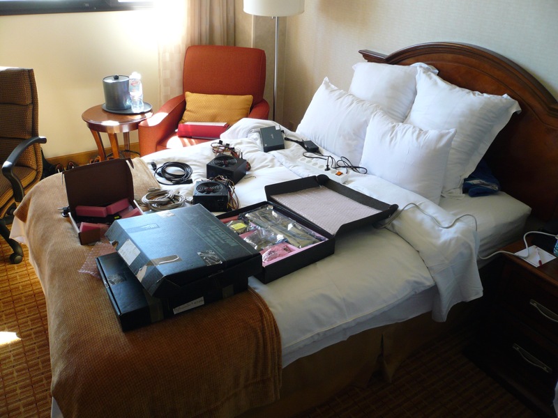 |
| Terrorists in a hotel room in San Francisco? Not really - in fact MIMO testbed preparations at its very beginning. Not a good time for a nap... |
 |
| Debugging a terminal of our real-time MIMO-OFDM testbed: A missing jumper related to received signal strength indication (RSSI) and frame synchronization at one RF board caused several hours of debugging work and impeded us from having dinner... |
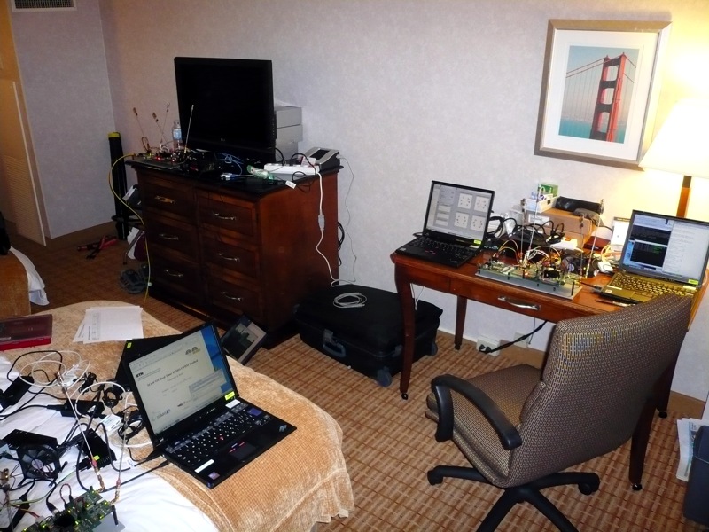 |
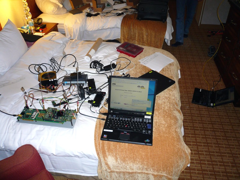
| By chance, our hotel room happened to change to a communications laboratory. Finally, everything is working as expected, great! Hmm, no more dinner... |
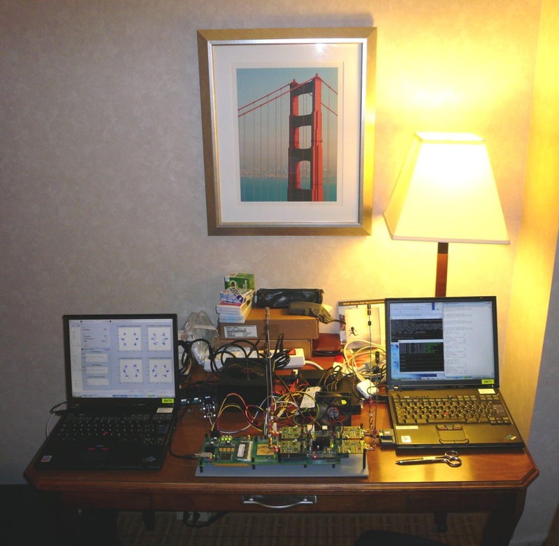 |
| Kind of a modern still life: Late-night testbed preparation activities in a hotel room in San Francisco, CA, USA, in order to get ready for next day's live demonstration contest. On the left laptop screen, you can see the constellation diagrams of four-stream MIMO wireless reception using QPSK modulation. The right laptop serves for observing and controlling the MIMO testbed and the embedded MAC by means of a terminal window connecting through RS232 to the embedded PowerPC CPU in the prototyping system. Moreover, the right laptop acts as server for video streaming using the VLC media player. The displayed MIMO testbed terminal constitutes the access point in this ad-hoc network. |
At the time of the ACM WinTech'08 live demonstration contest in September 2008, the MMSE-SQRD ASIC was not yet fully deployed to the testbed in order to demonstrate advanced MIMO detection schemes such as tree-search-based maximum likelihood (ML) or near-ML detection schemes. Nevertheless, linear MIMO detection in conjunction with four-stream MIMO transmission was fully operational and ready for live demonstration. In the end, we accomplished to win the second place in this live demonstration contest.
 |
| Testbed setup at the ACM WinTech'08 live demonstration contest in San Francisco, CA, USA, in late 2008: Three testbed terminals (1 access point, 2 stations) with 5 laptops demonstrating live video streaming and full Internet access using four-stream MIMO wireless communication. Well, during development and demonstration, I've seen different parts of the movie 'Office Space' for sure 100 times, but I never managed to see the entire movie at once from the beginning to the end... |
 |
| The terminal configured as access point of the real-time 4x4 MIMO-OFDM testbed at the WinTech'08 live demonstration contest in San Francisco, CA, USA. |
 |
| The testbed terminal configured as access point was attached through the yellow Gigabit Ethernet cable to a laptop running the VLC media player acting as server for live video streaming. Additionally, the laptop was also connected to the hotel's access point for providing full Internet access to the wireless MIMO network. |
 |
| One of the two testbed terminals configured as station and set up for receiving the live video stream. |
 |
| The testbed terminal configured as station for live video reception accompanied by two laptops: The left one served for playing the received video stream using the VLC media player. Guess, what movie? Yes, 'Office Space'. The laptop on the right displayed the corresponding statistics, e.g., instant and historic frame error rates, and showed actual constellation diagrams of received MIMO frames. |
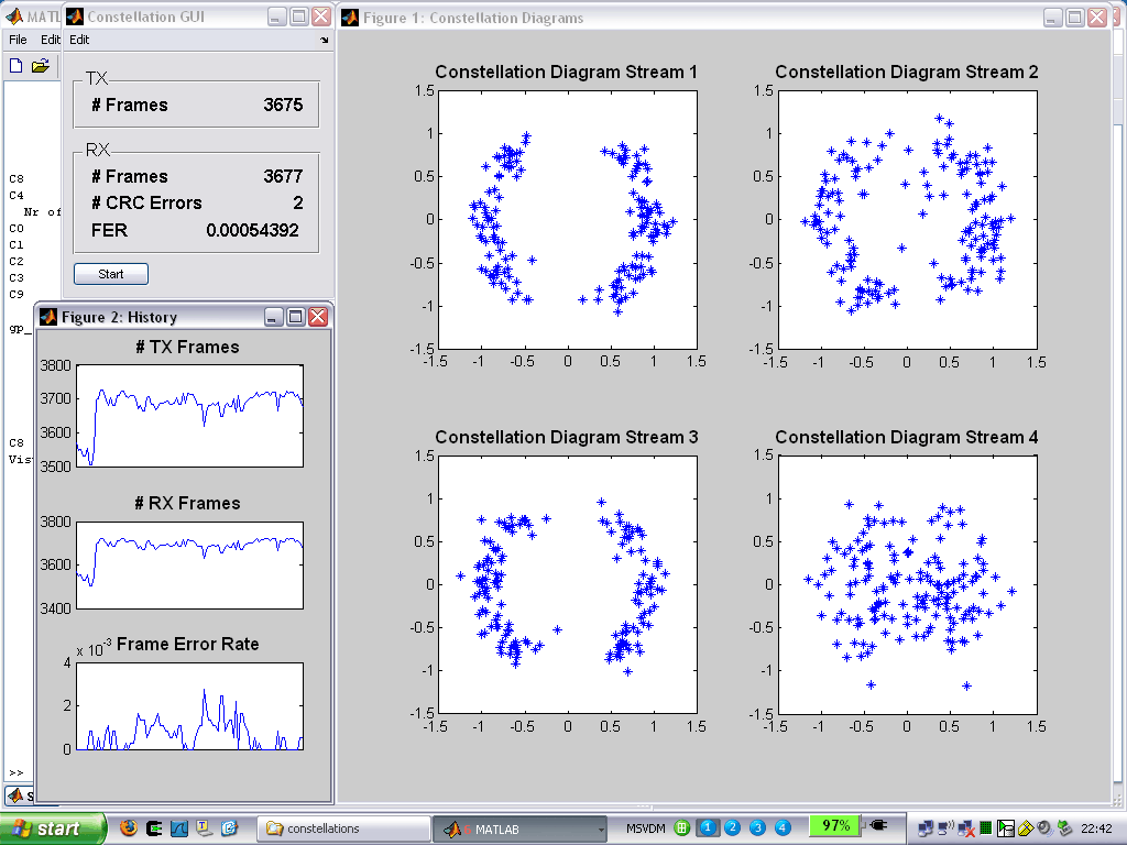 |
| Visualization of constellation diagrams of received MIMO frames, in this case four-stream MIMO reception with QPSK modulation, including number of transmitted and received frames and instant and historic frame error rates. Note that complex hardware-software systems deserve time and dedication in order to be put successfully into operation, as indicated by the system clock at the lower right side of the screen shot. |
At the time of the IEEE ISCAS'09 live demonstration contest in
May 2009, the MMSE-SQRD ASIC was completely deployed to the MIMO
testbed and fully operational in conjunction with different
tree-search-based MIMO detection schemes. As a consequence, we
were able to demonstrate for the first time advanced MIMO
detection schemes such as tree-search-based maximum likelihood
(ML) or near-ML MIMO detection. In the end, we have been awarded
the first place in this live demonstration contest.
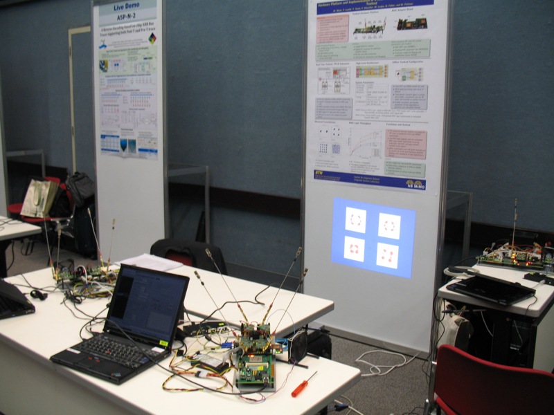 |
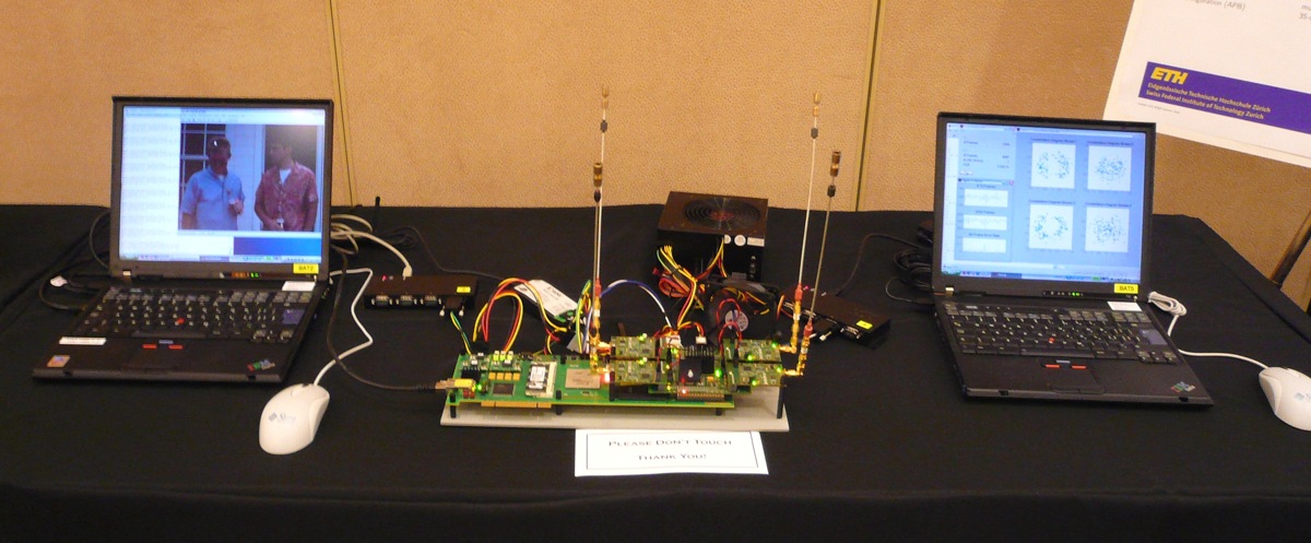
| Testbed setup at the IEEE ISCAS'09 live demonstration contest in Taipei, Taiwan, in May 2009: Three terminals of the real-time 4x4 MIMO-OFDM testbed demonstrated four-stream MIMO wireless communication including advanced tree-search-based MIMO detection schemes. The constellation diagrams of the received MIMO frames were instantly visualized with a beamer attached to one of the VGA ports of the MMSE-SQRD ASIC board. The picture shows four-stream MIMO communication with QPSK modulation. |
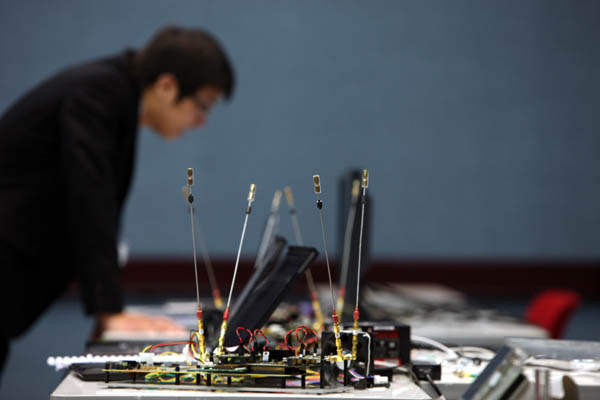 |
| One of the three MIMO testbed terminals at the IEEE ISCAS'09 live demonstration contest in Taipei, Taiwan. |
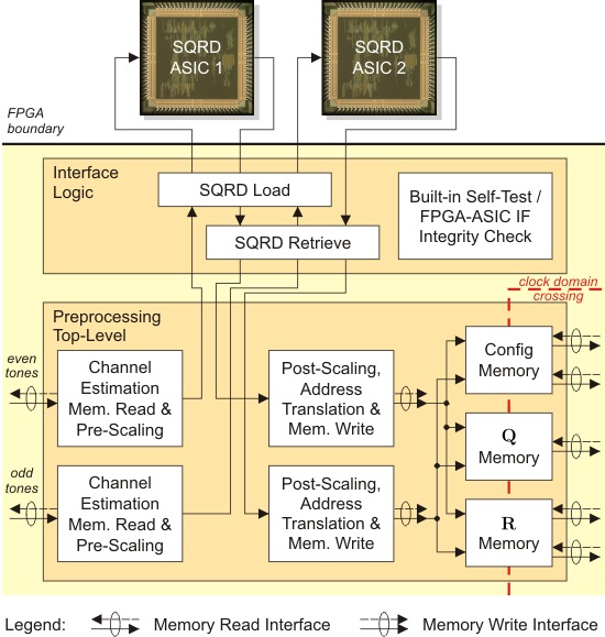 |
| Block diagram of the MIMO preprocessing architecture in the real-time MIMO-OFDM testbed. The SQRD-based preprocessing architecture is split into tree major parts: preprocessing top-level of the PHY logic, FPGA-ASIC interface logic, and channel matrix processing using two MMSE-SQRD ASICs. |
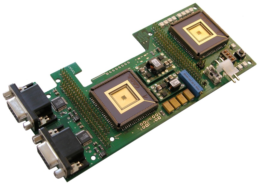 |
| Custom-designed printed circuit board for integration of the MMSE-SQRD ASIC in the real-time 4x4 MIMO-OFDM testbed. In addition, the board contains two video DACs with VGA output intended for being used in the MIMO testbed as versatile debugging infrastructure for different real-time aspects of MIMO PHY internals and as corresponding visualization resource for demonstration purposes. |
 |
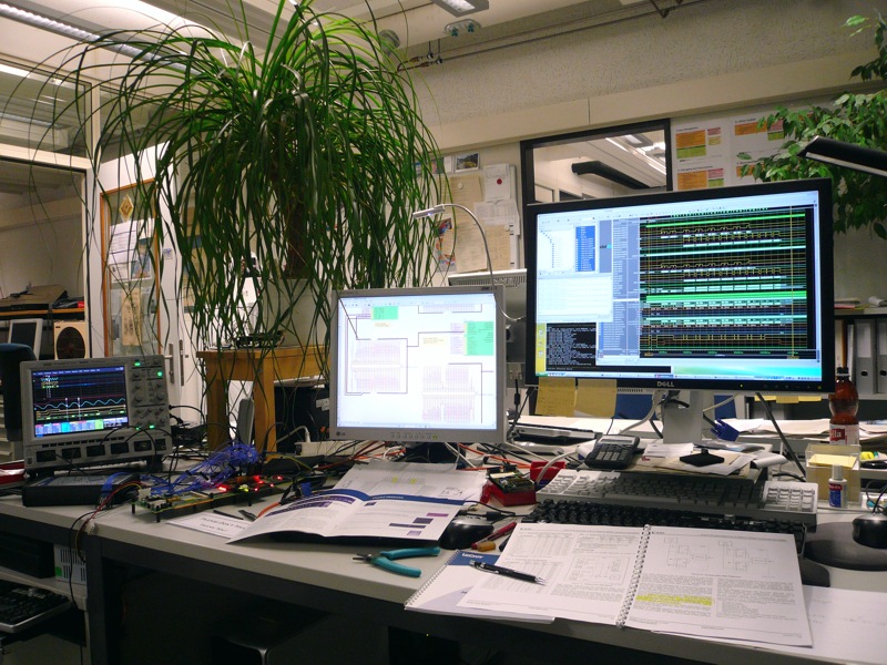
| Workspace showing the LeCroy WaveRunner 204 MXi oscilloscope for assessment of clock and control signals during initial bring-up of the communication interface between MMSE-SQRD ASICs and the XILINX Virtex-II Pro FPGA. |
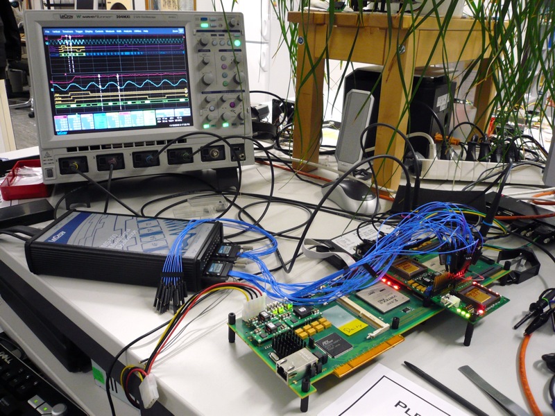 |
| Workspace showing the LeCroy WaveRunner 204 MXi oscilloscope and the LeCroy MS-500-36 mixed-signal extension for assessing electrical and timing aspects of the FPGA-ASIC interface during system-level deployment of the MIMO preprocessing block. This sophisticated and powerful technical solution from LeCroy greatly alleviated the challenging task of achieving system-level timing closure for the MIMO preprocessing block at a target clock frequency of 80 MHz, especially for the interface between ASICs and FPGA. |
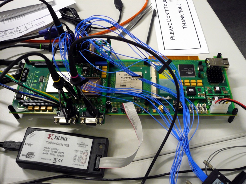 |
| Mixed-signal connections to the MMSE-SQRD ASIC interface on the MIMO prototyping platform. At the time of designing the PCB, I was not aware of the importance of convenient debugging access by means of a suitable high-density logic-analyzer connector. Instead, I simply relied on extended standard headers interfacing the MMSE-SQRD ASIC PCB with the VAMP board. The standard headers also allowed to accomplish the job, but correctly connecting approximately 27 unique logic-analyzer wires is tedious and much more error-prone, and finally lasted more than an hour... |
 |
| Workspace showing interface schematics in Altium Designer on the left screen and RTL simulation results in Mentor ModelSim as debugging reference on the right screen. |
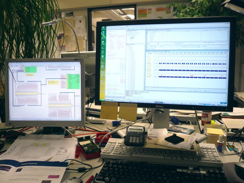 |
| Workspace showing interface schematics in Altium Designer on the left screen and XILINX ChipScope Pro in-system debugging results on the right screen. ChipScope Pro is a versatile debugging tool for the XILINX FPGA family by using synthesizable debugging blocks requiring FPGA-internal resources for capturing and storing digital signals. The captured signals are afterwards transferred and visualized on a PC. In principle, it is a low-cost logic analyzer specifically tailored to FPGA development without the needs for external connectivity to signals being debugged and the availability of costly logic analyzers. In short, ChipScope Pro represents a customizable debugging infrastructure for XILINX FPGAs and usually employs FPGA-internal memory resources for signal storage and the JTAG connection for control and data transfer. |
Last updated: 2013/06/01